Semiconductor Precision Laser Cutting Machine
Designed for stable processing of thin-sheet and micro-structure metal components
In semiconductor equipment and critical module manufacturing, dimensional stability, thermal impact control, and process repeatability are subject to extremely strict requirements.
Especially in thin-sheet structures and small precision part applications, cutting quality directly affects backend assembly yield and mass production stability.
Engineered around different process requirements and material characteristics, these precision laser cutting system configurations support high-accuracy machining, thin copper sheet processing, and stable mass production integration.
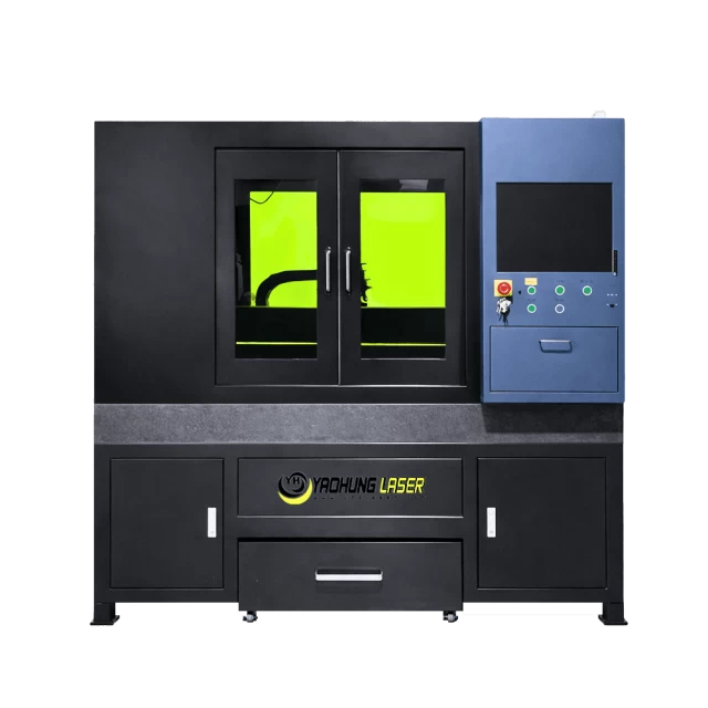
Precision Sheet Metal Laser Cutting Machine for Semiconductor Applications
Designed for the high-precision metal sheet processing commonly required in semiconductor equipment manufacturing, this configuration supports dimensional control, batch stability, and downstream assembly consistency. It is well suited for precision sheet metal parts and internal structural components used in semiconductor equipment.
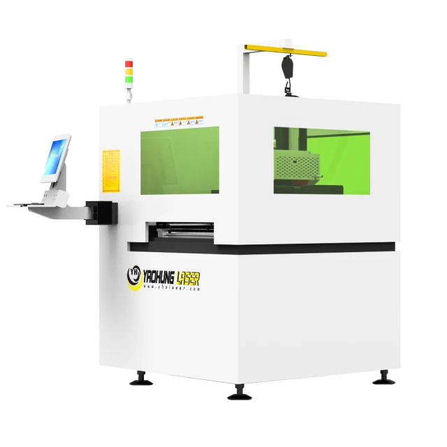
Precision Laser Cutting Machine for Semiconductor Thin Copper Sheets
Developed for thin copper conductive sheets, micro-structured conductive components, and other high-precision thin metal processing applications, this system can be configured according to workpiece characteristics and process requirements to improve cutting consistency, thermal impact control, and automation integration efficiency.
Applicable Process Scenarios
Based on material characteristics, precision requirements, and production line conditions, semiconductor precision laser cutting systems can support a wide range of high-specification metal processing applications, helping equipment manufacturers and supply chain partners enhance processing stability and implementation efficiency.
Thin Copper Conductive Sheet Cutting
Suitable for precision cutting of thin copper sheets and conductive materials, ensuring dimensional control, heat-affected zone management, and stable batch processing performance.
Precision Mask Components
Designed for mask structures and functional components requiring fine contours and tight dimensional tolerances, providing more stable precision cutting support.
Micro-Structure Metal Frames
Suitable for micro-scale metal components and precision frame structures, helping maintain cutting consistency and improve downstream assembly stability.
Internal Semiconductor Equipment Components
Applicable to internal metal components and critical parts in semiconductor equipment, supporting high-precision processing and automation integration requirements.
Precision Requirements in Semiconductor Laser Cutting Applications
Semiconductor manufacturing environments impose exceptionally strict requirements on dimensional stability, thermal impact control, and process repeatability in metal component fabrication. These challenges are particularly evident in thin-sheet structural parts, micro-scale precision components, and critical modules used in backend assembly processes.
Unlike general metal cutting applications that prioritize throughput or geometric completion, semiconductor precision cutting focuses on maintaining consistent machining outcomes across batches while minimizing deformation, heat-affected zones, and process variation. Achieving this level of stability requires not only advanced laser cutting capability, but also coordinated motion control architecture and integration readiness with automated production workflows.
Yao Hung Technology provides precision laser cutting configurations engineered around workpiece characteristics, tolerance requirements, and production takt conditions. By aligning cutting strategies with real manufacturing environments, equipment deployment can support stable yield performance, predictable quality outcomes, and scalable integration into semiconductor supply chain production systems.
Frequently Asked Questions
Semiconductor precision laser cutting is suitable for high-precision applications such as thin metal sheets, thin copper conductive parts, small precision components, and micro-structured metal parts.
It is especially recommended when tight dimensional tolerances, heat-affected zone control, batch consistency, and assembly stability are critical requirements.
General metal laser cutting focuses on shape completion and processing efficiency, while semiconductor precision laser cutting emphasizes dimensional stability, cutting consistency, heat-affected zone control, and process repeatability.
In applications involving thin materials, micro structures, and precision assembly components, system performance and integration capability directly affect production yield and stability.
Yes, but the process must be evaluated based on material thickness, reflectivity, contour complexity, and precision requirements.
In semiconductor applications, thin copper and conductive materials require strict control of thermal deformation, edge quality, and batch consistency, so customized precision laser cutting configurations are typically recommended.
When evaluating a semiconductor precision laser cutting solution, it is recommended to prepare the following information:
- Material type and thickness
- Part dimensions and contour complexity
- Tolerance and edge quality requirements
- Expected production volume and batch consistency
- Automation requirements such as loading/unloading or production line integration
These factors directly influence system configuration, motion control design, and overall process planning, and are essential for accurate solution evaluation.
Process Optimization through Customized Semiconductor Laser Cutting
From concept to configuration — We build it your way.
Discover Tailored Integration Solutions